SDIO wifi Marvell8801/Marvell88w8801 介绍(二) ---- SDIO协议介绍-程序员宅基地
技术标签: SDIO Marvelll88w8801 marvell8801 # Marvell8801 SDIO WIFI WIFI
代码工程的GITHUB连接:点进进入GITHUB仓库
https://github.com/sj15712795029/stm32f1_marvell88w8801_marvell8801_wifi
点击购买Marvell8801开发板
Marvell自己实现驱动系列文章分为几篇介绍:
SDIO wifi Marvell8801/Marvell88w8801 介绍(一) ---- 芯片介绍
SDIO wifi Marvell8801/Marvell88w8801 介绍(二) ---- SDIO协议介绍
SDIO wifi Marvell8801/Marvell88w8801 介绍(三) ---- 寄存器介绍
SDIO wifi Marvell8801/Marvell88w8801 介绍(四) ---- 命令/事件/数据格式
SDIO wifi Marvell8801/Marvell88w8801 介绍(五) ---- TLV
SDIO wifi Marvell8801/Marvell88w8801 介绍(六) ---- 实现初始化功能
SDIO wifi Marvell8801/Marvell88w8801 介绍(七) ---- 实现搜索功能
SDIO wifi Marvell8801/Marvell88w8801 介绍(八) ---- 实现STA功能
SDIO wifi Marvell8801/Marvell88w8801 介绍(九) ---- 实现AP功能
SDIO wifi Marvell8801/Marvell88w8801 介绍(十) ---- 移植TCP/IP协议栈LWIP
SDIO wifi Marvell8801/Marvell88w8801 介绍(十一) ---- 自己编写LWIP没有的DHCP server
SDIO wifi Marvell8801/Marvell88w8801 介绍(十二) ---- MQTT介绍
SDIO wifi Marvell8801/Marvell88w8801 介绍(十三) ---- 百度云操作说明
SDIO wifi Marvell8801/Marvell88w8801 介绍(十四) ---- 上位机STA操作/代码
SDIO wifi Marvell8801/Marvell88w8801 介绍(十五) ---- 上位机AP操作/代码
SDIO wifi Marvell8801/Marvell88w8801 介绍(十六) ---- 上位机UDP操作/代码
SDIO wifi Marvell8801/Marvell88w8801 介绍(十七) ---- 上位机TCP操作/代码
SDIO wifi Marvell8801/Marvell88w8801 介绍(十八) ---- 上位机PING操作/代码
SDIO wifi Marvell8801/Marvell88w8801 介绍(十九) ---- 上位机云服务器(百度云)操作/代码
每篇更新打开专栏可以看到:打开Marvell8801/Marvell8801 专栏
在介绍SDIO协议之前,我们来看下Wi-Fi市面上的种类
1. WI-FI接口介绍
市面上大致有这几种Wi-FI,其中优缺点也是我个人简介,大家一看就好,至于有不同意见,可以交流
1)UART WIFI,以ESP8266为代表,主要实现方式是芯片内集成了wifi driver+tcp/ip protocol+rtos+memory IC等等,让你可以直接AT命令控制芯片
优点:使用便利,开发者不需要懂WIFI driver,TCP/IP protocol,RTOS的概念
缺点:功能受限,可定制化比较低,需要外挂一个MCU
另外,ESP8266也分为AT板和SDK板,SDK也可以克服以上缺点,但是我没有使用过SDK,所以不能胡说错误的引导你们
2)SDIO WIFI
3)USB WIFI
其中SDIO和USB市面上就比较多了,大部分的Wifi芯片都是以上两种接口,Marvell88w8801支持USB2.0和SDIO2.0 ,USB wifi大家看名字应该就能想象到时什么东西,就是类似于一个USB dongle,下图模样

SDIO WIFI我们后续会介绍,所以大家不要急
4)PCIE WIFI如图
5)OPENWRT WIFI
由于我没有做过这个,所以不做评论
2. SDIO协议介绍
做一个简短性的话语总结,SDIO有分为FUNC的概念,你可以把FUNC比作功能区,FUNC0是每个SDIO card必须实现的,FUNC1~7是可选存在的,一般的WIFI card会实现FUNC1,在每个FUNC中又会有寄存器的概念,FUNC0中的寄存器地址是SDIO协议规定,FUNC1~FUNC7中的寄存器地址是vendor(芯片厂商)去实现的,所以要访问一个地址的数据,首先要告知FUNC,然后再告知register address,整个大背景在这,好啦,SDIO讲解到此为止~哈哈,玩笑啦,带着这些去读下面的内容吧,会让你更容易理解
2.1 SDIO硬件接口介绍
SDIO设备的硬件操作接口有3种方式:
A、 SPI mode;
B、 SD 1-bit mode;
C、 SD 4-bit mode;
这3种方式的硬件接口及管脚定义如下面图、表:

图1 SDIO硬件接口(连接了2组sdio设备)
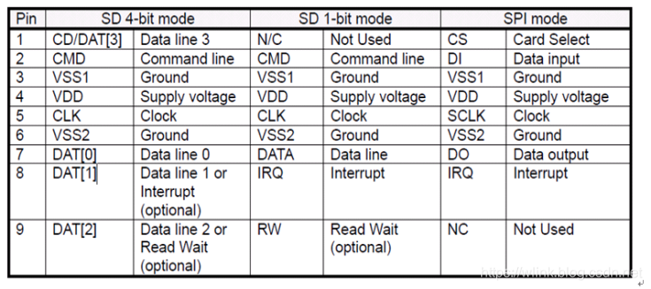
表1 SDIO各种模式管脚对应关系
本文不对SPI mode的相关内容介绍,有关SPI mode的内容不做过多说明。
2.2 SDIO 概念介绍
2.2.1 Common I/O Area (CIA)
The Common I/O Area (CIA) shall be implemented on all SDIO cards. The CIA is accessed by the host via I/O reads and writes to function 0. The registers within the CIA are provided to enable/disable the operation of the I/O function(s), control the generation of interrupts and optionally load software to support the I/O
functions. The registers in the CIA also provide information about the function(s) abilities and requirements. There are three distinct register structures supported within the CIA. They are:
1) Card Common Control Registers (CCCR)
2)Function Basic Registers (FBR)
3)Card Information Structure (CIS)
如图所示,就是FUNC0的CIA
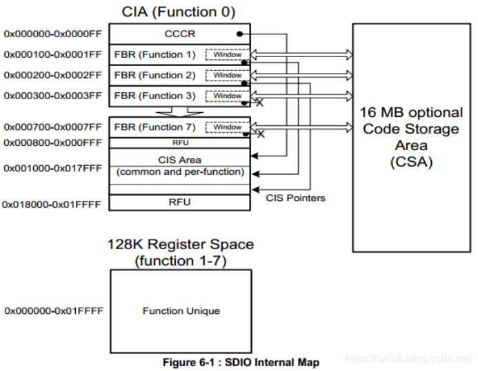
下面我们来一一介绍CCCR,FBR,CIS
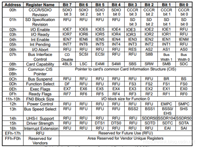
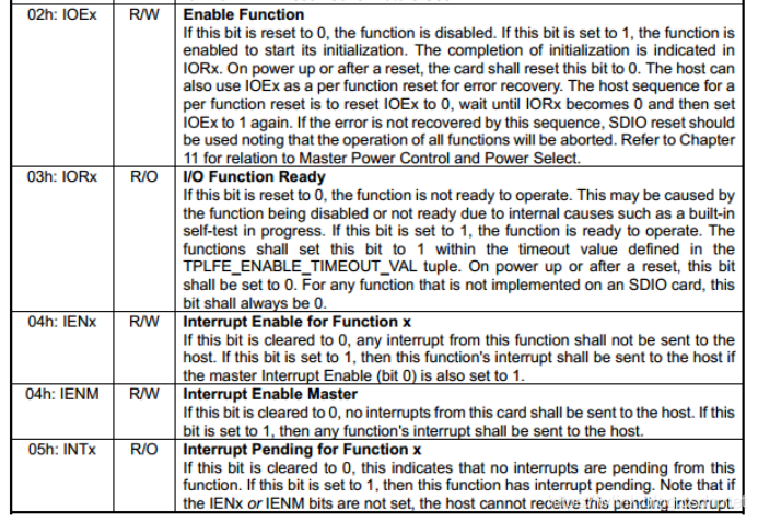
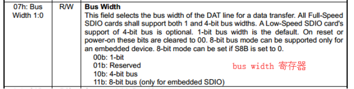
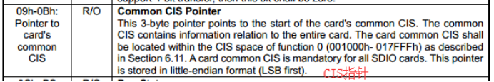
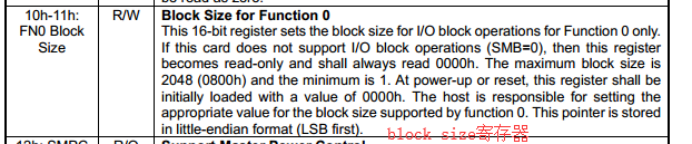
Card Common Control Registers (CCCR):CCCR说白了就是FUNC0的一些寄存器,地址和功能如下,另外,如果把所有的都列出内容实在太多,在这里只是列举一些重要的,如果想获取所有的功能,请自行参考SDIO协议:
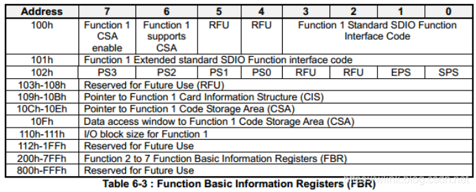
2.2.2 Function Basic Registers (FBR)
In addition to the CCCR, each supported I/O function has a 256-byte area used to allow the host to quickly determine the abilities and requirements of each function, enable power selection for each function and to enable software loading. The address of this area is from 00n00h to 00nFFh where n is the function number (1 to 7). This per-function area is structured as follows:
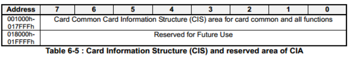
2.2.3 Card Information Structure (CIS)
The Card Information Structure provides more complete information about the card and the individual functions. The CIS is the common area to read information about all I/O functions that exist in a card. The design is based on the PC Card16 design standardized by PCMCIA. All cards that support I/O shall have a common CIS and a CIS for each function. The CIS is accessed by reads to a fixed area as shown in Table 6-5 This one area serves the card as a Common CIS and also as the storage area for each function. The common area and each function have a pointer to the start of its CIS within this memory space.
另外,CIS是tuple实行存在的,所以如果读出来需要自己解析,在后面小节会抽出一章节讲解tuple.
2.2.4 SDIO 命令/相应介绍
SDIO spec中有提到几点SDIO card必须要实现的以及可选要实现的命令,如下
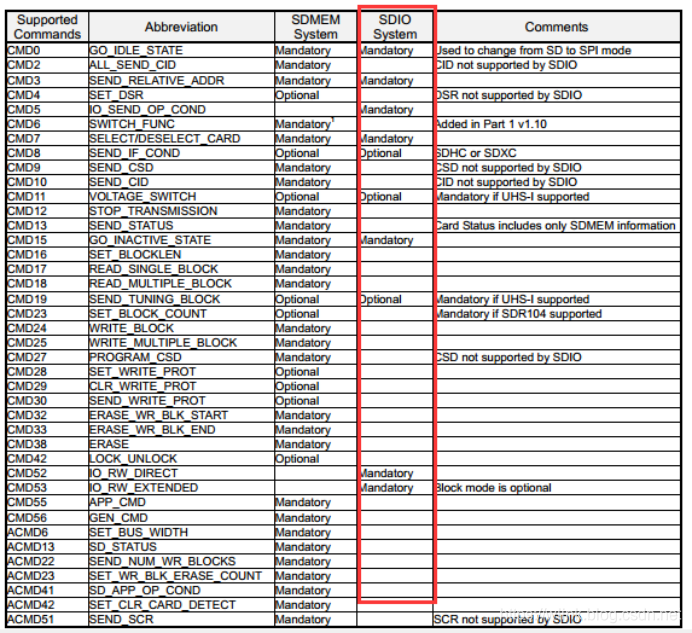
必须要实现的有:CMD0,CMD3,CMD5,CMD7,CMD15,CMD52,CMD53
可选实现的有:CMD8,CMD11,CMD15
Marvell88w8801的datasheet上也有说这颗芯片支持的CMD,算是把强制需要support的都做了,选择支持的一个没做,哈哈
但是我们一般用到的有CMD0,CMD3,CMD5,CMD7,CMD52,CMD53,所以以这几个命令来做简短说明
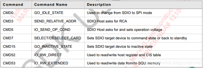
1)CMD0:用于从SDIO mode切换到SPI mode
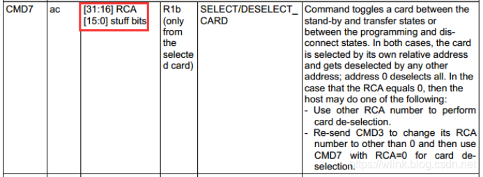
2)CMD3:询问相对可用地址,response是R6

代码如下:
/******************************************************************************
 *	函数名:	hw_sdio_cmd3
 * 参数:  	para(IN)		-->发送cmd3的参数
 			resp			-->cmd3的返回值
 * 返回值: 	返回执行结果
 * 描述:	发送cmd3
******************************************************************************/
static uint8_t hw_sdio_cmd3(uint32_t para,uint32_t *resp)
{

    uint8_t error_status;
    uint32_t response;
    SDIO_CmdInitTypeDef SDIO_CmdInitStructure;

    SDIO_CmdInitStructure.SDIO_Argument = para;
    SDIO_CmdInitStructure.SDIO_CmdIndex = SDIO_CMD3;
    SDIO_CmdInitStructure.SDIO_Response = SDIO_Response_Short;
    SDIO_CmdInitStructure.SDIO_Wait = SDIO_Wait_No;
    SDIO_CmdInitStructure.SDIO_CPSM = SDIO_CPSM_Enable;
    SDIO_SendCommand(&SDIO_CmdInitStructure);

    /* 等待发送完成 */
    while (SDIO_GetFlagStatus(SDIO_FLAG_CMDACT) == SET);
    error_status = hw_sdio_check_err();

    if (HW_ERR_OK != error_status)
    {

        return error_status;
    }

    /* 获取到response的结果 */
    response = SDIO_GetResponse(SDIO_RESP1);
    if (resp)
    {

        *resp = response;
    }

    return (error_status);
}
R6的格式格式为,只有红框内的数据才是软件可以获取的,其他的都是交于硬件去搞定
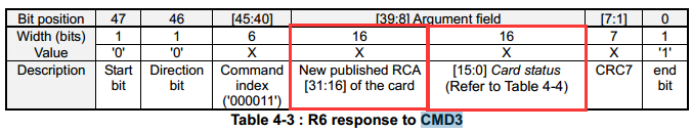
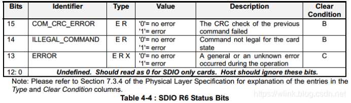
Bit 0~15是card status,如下图
Bit 16~31就是我们获取的相对地址,需要软件解析出来,搭配CMD7来使用
解析代码如下:
/******************************************************************************
 *	函数名:	hw_sdio_parse_r6
 * 参数:  	r6(IN)			-->R6的入参
 			rca(OUT)		-->rca的返回值
 * 返回值: 	返回执行结果
 * 描述:	解析R6的response
******************************************************************************/
static uint8_t hw_sdio_parse_r6(uint32_t r6,uint32_t *rca)
{

    HW_ENTER();
    if(rca)
    {

        *rca = RCA_IN_R6(r6);
        HW_LEAVE();
        return HW_ERR_OK;
    }
    HW_LEAVE();
    return HW_ERR_SDIO_INVALID_PARA;
}
3)CMD5, It is used to inquire about the voltage range needed by the I/O card.命令格式如下
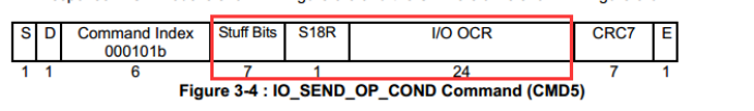
Stuff Bits: Not used, shall be set to 0.
S18R: Switching to 1.8V Request
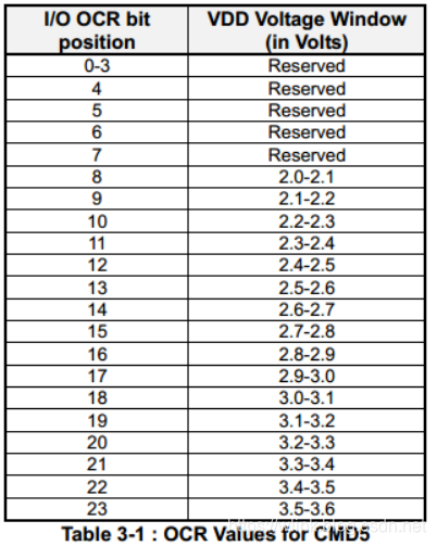
I/O OCR: Operation Conditions Register. The supported minimum and maximum values for VDD. The layout of the OCR is shown in Table 3-1. Refer to Section 4.10.1 for additional information
OCR如下图
CMD5的response如下图:
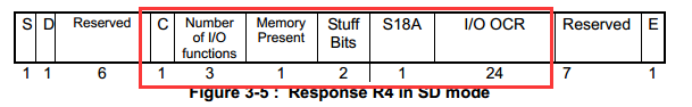
C: Set to 1 if Card is ready to operate after initialization
Number of I/O Functions: Indicates the total number ofI/O functions supported by this card. The range is 0-7. Note that the common area present on all I/O cards at Function 0 is not included in this count. The I/O functions shall be implemented sequentially beginning at function 1.
Memory Present: Set to 1 if the card also containsSD memory. Set to 0 if the card is I/O only.
S18A: Switching to 1.8V Accepted (Supported in SD mode only)
I/O OCR: Operation Conditions Register.
代码如下:
/******************************************************************************
 *	函数名:	hw_sdio_cmd5
 * 参数:  	para(IN)			-->入参
 			resp(OUT)			-->返回值
 			retry_max(IN)		-->最大尝试次数
 * 返回值: 	返回执行结果
 * 描述:	发送cmd5
******************************************************************************/
static uint8_t hw_sdio_cmd5(uint32_t para,uint32_t *resp,uint32_t retry_max)
{

    uint32_t index;
    uint32_t response;
    uint8_t error_status;
    SDIO_CmdInitTypeDef SDIO_CmdInitStructure;

    HW_ENTER();
    SDIO_CmdInitStructure.SDIO_Argument = para;
    SDIO_CmdInitStructure.SDIO_CmdIndex = SDIO_CMD5 ;
    SDIO_CmdInitStructure.SDIO_Response = SDIO_Response_Short;
    SDIO_CmdInitStructure.SDIO_Wait = SDIO_Wait_No;
    SDIO_CmdInitStructure.SDIO_CPSM = SDIO_CPSM_Enable;
    for (index = 0; index < retry_max; index++)
    {

        SDIO_SendCommand(&SDIO_CmdInitStructure);
        /* 等待发送完成 */
        while (SDIO_GetFlagStatus(SDIO_FLAG_CMDACT) == SET);
        error_status = hw_sdio_check_err();

        if (HW_ERR_OK != error_status)
        {

            continue;
        }
        response = SDIO_GetResponse(SDIO_RESP1);

        /* 判断是否OK */
        if(C_IN_R4(response))
        {

            if (resp)
            {

                *resp = response;
            }
            break;
        }
    }

    HW_LEAVE();
    return error_status;
}
4)CMD7
代码如下:
/******************************************************************************
 *	函数名:	hw_sdio_cmd7
 * 参数:  	para(IN)			-->入参
 			resp(OUT)			-->返回值
 * 返回值: 	返回执行结果
 * 描述:	发送cmd7
******************************************************************************/
static uint8_t hw_sdio_cmd7(uint32_t para,uint32_t *resp)
{

    uint8_t error_status;
    uint32_t response;
    SDIO_CmdInitTypeDef SDIO_CmdInitStructure;

    HW_ENTER();
    /* Send CMD7 SDIO_SEL_DESEL_CARD */
    SDIO_CmdInitStructure.SDIO_Argument = para;
    SDIO_CmdInitStructure.SDIO_CmdIndex = SDIO_CMD7;
    SDIO_CmdInitStructure.SDIO_Response = SDIO_Response_Short;
    SDIO_CmdInitStructure.SDIO_Wait = SDIO_Wait_No;
    SDIO_CmdInitStructure.SDIO_CPSM = SDIO_CPSM_Enable;
    SDIO_SendCommand(&SDIO_CmdInitStructure);

    /* 等待发送完成 */
    while (SDIO_GetFlagStatus(SDIO_FLAG_CMDACT) == SET);
    error_status = hw_sdio_check_err();

    if (HW_ERR_OK != error_status)
    {

        return error_status;
    }
    /* 获取返回结果 */
    response = SDIO_GetResponse(SDIO_RESP1);
    if (resp)
    {

        *resp = response;
    }

    HW_ENTER();
    return (error_status);
}
5)CMD52:CMD52是一个使用频率很高的CMD,主要是用于读写SDIO的寄存器的命令
The IO_RW_DIRECT is the simplest means to access a single register within the total 128K of register space in any I/O function, including the common I/O area (CIA). This command reads or writes 1 byte using only 1 command/response pair. A common use is to initialize registers or monitor status values for I/O functions. This command isthe fastest means to read or write single I/O registers, as it requires only a single command/response pair.
命令格式如下,红框内饰软件需要实现的东西,其他的交给硬件:
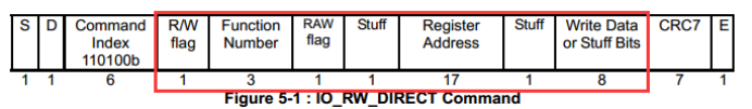
R/W Flag: This bit determines the direction of the I/O operation. If this bit is 0, this command
shall read data from the SDIO card at the address specified by the Function Number and the Register Address to the host. The data byte is returned in the response, R5. If this bit is set to 1, the command shall write the bytes in the Write Data field to the I/O location addressed by the Function Number and the Register Address. If the RAW flag is 0, then the data inthe register that was written shall be read and that value returned in the response.
RAW Flag: The Read after Write flag. If this bit isset to 1 and the R/W flag is set to 1, then the
command shall read the value of the register after the write. This is useful to allow writing to a control register and reading the status at the same address. If this bit is cleared, the value returned in the R5 response shall be the same as the write data in the command. If this bit is set, the data field of the R5 response shall contain the value read from the addressed register after the write operation.
Function Number: The number of the function within the I/O card you wish to read or write. Note that function 0 selects the common I/O area (CIA).
Register Address: This is the address of the byte ofdata inside of the selected function to read or write. There are 17 bits of address available so the register is located within the first 128K
(131,072) addresses of that function.
Write Data/Stuff Bits: For a direct write command (R/W=1),this is the byte that iswritten to the selected address. For a direct read (R/W=0), this field is not used and shall be set to 0
响应类型:
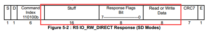
Stuff Bits Not used, shall be set to 0
Response Flags 8 Bits of flag data indicating the status of the SDIO card. Table 5-1 shows the format of these flag bits.
Read or Write Data: For an I/O write (R/W=1) with the RAW Flag set (RAW=1) this field shall contain the value read from the addressed register afterthe write of the data contained in the
command. Note that in this case, the read-back data may not be the same as the data written to the register, depending on the design of the hardware. For an I/O write with the RAW bit=0, the SDIO function shall notdo a read after write operation, and the data in this field shall be identical to the data byte in the write command. For an I/O read (R/W=0), the actual value read from that I/O location is returned in this field.
代码如下:
/******************************************************************************
 *	函数名:	hw_sdio_cmd52
 * 参数:  	write(IN)			-->执行操作,read or write
 			func_num(IN)		-->func的编号
 			address(IN)		-->address地址
 			para(IN)			-->要写的参数
 			resp(OUT)			-->读要返回的数据
 * 返回值: 	返回执行结果
 * 描述:	执行CMD52的动作
******************************************************************************/
uint8_t hw_sdio_cmd52(uint8_t write,uint8_t func_num,uint32_t address,uint8_t para,uint8_t *resp)
{

    uint8_t error_status;
    uint8_t response;
    SDIO_CmdInitTypeDef SDIO_CmdInitStructure;

    SDIO_CmdInitStructure.SDIO_Argument = write ? 0x80000000 : 0x00000000;
    SDIO_CmdInitStructure.SDIO_Argument |= func_num << 28;
    SDIO_CmdInitStructure.SDIO_Argument |= (write && resp) ? 0x08000000 : 0x00000000;
    SDIO_CmdInitStructure.SDIO_Argument |= address << 9;
    SDIO_CmdInitStructure.SDIO_Argument |= para;

    SDIO_CmdInitStructure.SDIO_CmdIndex = SDIO_CMD52;
    SDIO_CmdInitStructure.SDIO_Response = SDIO_Response_Short;
    SDIO_CmdInitStructure.SDIO_Wait = SDIO_Wait_No;
    SDIO_CmdInitStructure.SDIO_CPSM = SDIO_CPSM_Enable;

    SDIO_SendCommand(&SDIO_CmdInitStructure);
    /* 等待发送完成 */
    while (SDIO_GetFlagStatus(SDIO_FLAG_CMDACT) == SET);
    error_status = hw_sdio_check_err();

    if (HW_ERR_OK != error_status)
    {

        return  HW_ERR_SDIO_CMD52_FAIL;
    }

    response = SDIO_GetResponse(SDIO_RESP1) & 0xff;
    if((!write) && resp)
    {

        *resp = response;
    }
    return  HW_ERR_OK;
}
6)CMD53:同样是一个高频使用的CMD,主要用于对某一个地址进行多数据写入或者多数据读出的CMD,此命令分为两种模式:block mode和byte mode,block mode必须是写入或者读出block size整数倍的数据,byte mode是可以写入或者读出任意大小的数据
命令格式:
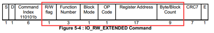
R/W Flag: This bit determines the direction of the I/O operation. If this bit is 0, this command
reads data from the SDIO card at the address specified by the Function Number and the Register Address to the host. The read data shall be returned on the DAT[x] lines. If this bit is set to 1, the command shall write the bytes from the DAT[x] lines to the I/O location addressed by the Function Number and the Register Address.
Function Number: The number of the function within the I/O card you wish to read or write. Note that function 00h selects the common I/O area (CIA).
Block Mode (Optional) this bit, if set to 1, indicates that the read or write operation shall be performed on a block basis, rather than the normal byte basis. If this bit is set, the Byte/Block count value shall contain the number of blocks to be read/written. The block size for functions 1-7 is set by writing the block size to the I/Oblock size register in the FBR (Refer to Table 6-3 and Table 6-4). The block size for function 0 is set by writing to the FN0 Block Size register in the CCCR. Card and hostsupport of the block I/O mode is optional. The host can determine if a card supports block I/O by reading the Card supports MBIO bit (SMB) in the CCCR (Refer to Table 6-2). The block size used when Block Mode = 1 and the maximum byte count per command used when
Block Mode = 0 can be read from the CIS inthe tuple TPLFE_MAX_BLK_SIZE (Refer to Section 16.7.4) on a per-function basis.
OP code Defines the read/write operation as described in Table 5-2
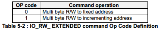
• OP Code 0 is used to read or write multiplebytes of data to/from a single I/O register address. This command is useful when I/O data is transferred using a FIFO inside of the I/O card. In this case, multiple bytes of data are transferred to/from a single register address. For this operation, the address of the register is set into the Register Address field. Data is transferred on the DAT[0] orDAT[3:0] lines as defined for SD memory cards.
•OP Code 1 is used to read or write multiple bytes of data to/from an I/O register address that increment by 1 after each operation. This command is used when large amounts of I/O data exist within the I/O card ina RAM like data buffer. In this operation,the start address is loaded into the Register Address field. The first operation occurs at that address within the I/O card. The next operation shall occur at address+1 with the address incrementing by 1 until the operation has completed. As with OP Code 0, the number of bytes is set in the Byte Count field of the command.
Register Address: Start Address of I/O register to read or write. Range is [1FFFFh:0]
Byte/Block Count :If the command is operating on bytes (Block Mode = 0), this field contains the number of bytes to read or write. A value of 000h shall cause 512 bytes to be read or written.

If the command is in block mode (Block Mode=1), the Block Count field specifies the number of Data Blocks to be transferred following this command. A value of 000h indicates that the count set to infinite. In this case, the I/O blocks shall be transferred until the operation is aborted by writing to the I/O abort function select bits (ASx) in the CCCR (Refer to Table 6-1 and Table 6-2). Table 5-3 shows the relationship between the value in the command and the actual number of bytes transferred.
代码如下:
/******************************************************************************
 *	函数名:	hw_sdio_cmd52
 * 参数:  	write(IN)			-->执行操作,read or write
 			func_num(IN)		-->func的编号
 			address(IN)			-->address地址
 			incr_addr(IN)		-->地址是否累加
 			buf(IN/OUT)			-->如果操作是写,那么此参数就是要write的buffer
 									如果操作是读,那么此参数就是read返回的buffer
 			size(IN)			-->读或者写的size
 * 返回值: 	返回执行结果
 * 描述:	执行CMD53的动作
******************************************************************************/
uint8_t hw_sdio_cmd53(uint8_t write, uint8_t func_num,uint32_t address, uint8_t incr_addr, uint8_t *buf,uint32_t size)
{

    uint16_t func_cur_blk_size;

    if((phw_sdio_core->func)[func_num])
    {

        func_cur_blk_size = (phw_sdio_core->func)[func_num]->cur_blk_size;
        if(func_cur_blk_size == 0)
        {

            return HW_ERR_SDIO_BLK_SIZE_ZERO;
        }
    }
    else
    {

        return HW_ERR_SDIO_INVALID_FUNC_NUM;
    }

    if(write)
    {

        /* CMD53 write */
        hw_sdio_cmd53_write(func_num,address,incr_addr,buf,size,func_cur_blk_size);
    }
    else
    {

        /* CMD53 read */
        hw_sdio_cmd53_read(func_num,address,incr_addr,buf,size,func_cur_blk_size);
    }

    return  HW_ERR_OK;
}
2.2.5 SDIO init介绍
关于SDIO init流程,我们先以一个图示介绍,由于此图示是结合SD memroy card一起的,所以我们在图中以箭头表示流程,如图所示:
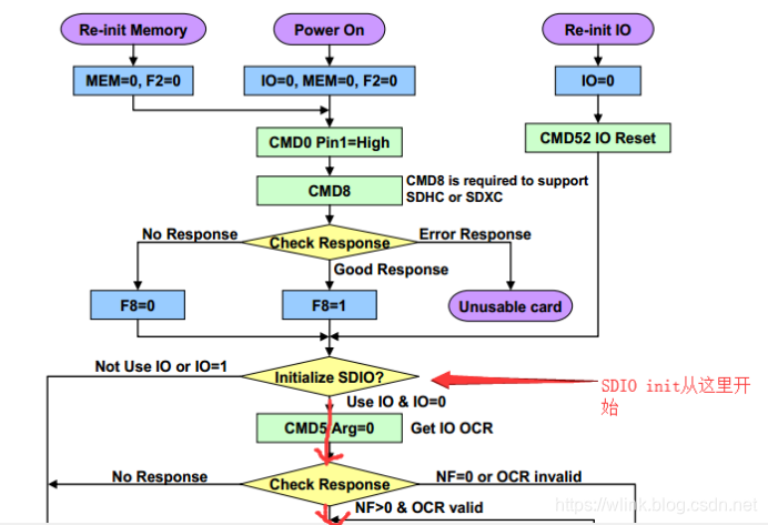
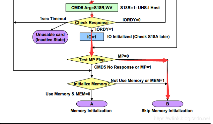
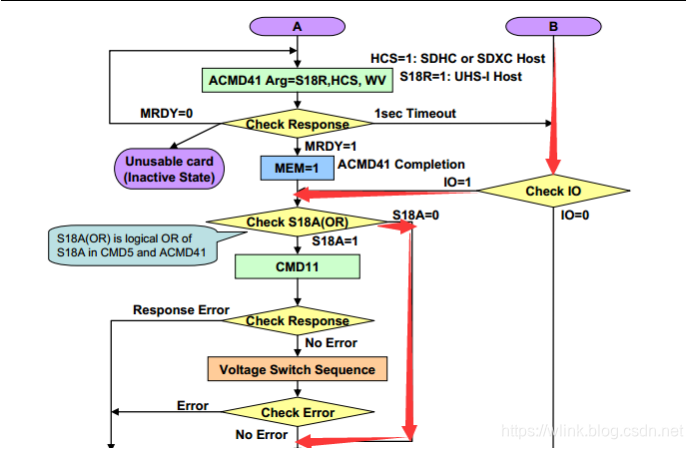
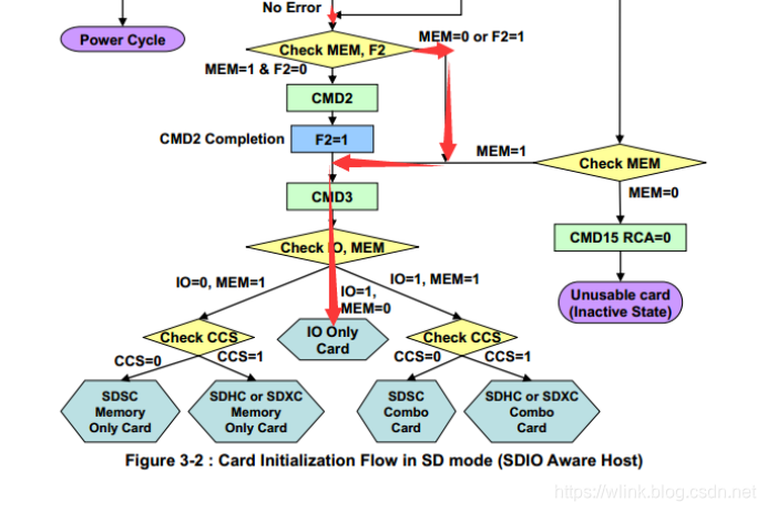
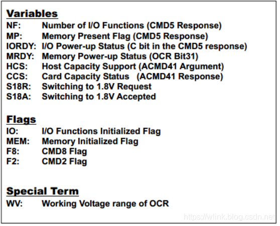
其中有一些术语如图所示:
大概过程如下:
1)发送CMD5没有参数,主要用于获取OCR的范围
2)FUNC的数目和OCR如果合法那么就重新发送CMD5,带着OCR的参数
3)得到RESPONSE后,查看MP的filed,正常来说SDIO MP应该为0,所以走B case
4)B case下IO为1,并且S18为0,所以直接走CMD3,然后是IO=1,MEM=0,也就是SDIO整个初始化完毕,但是SDIO还有一些其他选项需要做,比如选择SDIO设备,读取一些CCCR的信息,切换SDIO bus width,提高SDIO CLK,解析CIS,设置BLOCK size之类的,下面我贴出我在STM32写的代码,仅供参考流程,这部分也在我的GITHUB能找到
/******************************************************************************
 *	函数名:	hw_sdio_init
 * 参数:  		NULL
 * 返回值: 	返回执行结果
 * 描述:		SDIO init
 				pin脚分配
 				PC8->SDIO D0 PC9->SDIO D1 PC10->SDIO D2 PC11->SDIO D3
 				PC12->SDIO CLK
 				PD2->SDIO CMD
******************************************************************************/
uint8_t hw_sdio_init()
{

    uint32_t rca;
    uint8_t func_index;
    uint32_t cmd3_para;
    uint32_t cmd3_resp;
    uint32_t cmd5_para;
    uint32_t cmd5_resp;
    uint32_t cmd7_para;
    uint32_t cmd7_resp;

    GPIO_InitTypeDef GPIO_InitStructure;
    SDIO_InitTypeDef SDIO_InitStructure;
    //NVIC_InitTypeDef NVIC_InitStructure;

    HW_ENTER();
    hw_chip_reset();
    hw_sdio_core_init();
    /* 使能GPIO C/D的RCC时钟 */
    RCC_APB2PeriphClockCmd(RCC_APB2Periph_GPIOC | RCC_APB2Periph_GPIOD, ENABLE);
    /* 使能SDIO RCC时钟*/
    RCC_AHBPeriphClockCmd(RCC_AHBPeriph_SDIO, ENABLE);
    /* 使能DMA2时钟,SDIO的DMA在DMA2 CHANNEL 4 */
    RCC_AHBPeriphClockCmd(RCC_AHBPeriph_DMA2, ENABLE);

    /* 设置推挽复用 */
    GPIO_InitStructure.GPIO_Pin = GPIO_Pin_8 | GPIO_Pin_9 | GPIO_Pin_10 | GPIO_Pin_11 | GPIO_Pin_12;
    GPIO_InitStructure.GPIO_Speed = GPIO_Speed_50MHz;
    GPIO_InitStructure.GPIO_Mode = GPIO_Mode_AF_PP;
    GPIO_Init(GPIOC, &GPIO_InitStructure);

    GPIO_InitStructure.GPIO_Pin = GPIO_Pin_2;
    GPIO_Init(GPIOD, &GPIO_InitStructure);

    /* SDIO初始化,CLK:400KHZ,数据宽度:1 bus */
    SDIO_DeInit();
    /* HCLK = 72MHz, SDIOCLK = 72MHz, SDIO_CK = HCLK/(178 + 2) = 400 KHz */
    SDIO_InitStructure.SDIO_ClockDiv = SDIO_CLK_400KHZ;
    SDIO_InitStructure.SDIO_ClockEdge = SDIO_ClockEdge_Rising ;
    SDIO_InitStructure.SDIO_ClockBypass = SDIO_ClockBypass_Disable;
    SDIO_InitStructure.SDIO_ClockPowerSave = SDIO_ClockPowerSave_Disable;
    SDIO_InitStructure.SDIO_BusWide = SDIO_BusWide_1b;
    SDIO_InitStructure.SDIO_HardwareFlowControl = SDIO_HardwareFlowControl_Disable;
    //SDIO_InitStructure.SDIO_HardwareFlowControl = SDIO_HardwareFlowControl_Enable;
    SDIO_Init(&SDIO_InitStructure);

    /* 设置为SDIO I/O模式 */
    SDIO_SetSDIOOperation(ENABLE);
    /* Set Power State to ON */
    SDIO_SetPowerState(SDIO_PowerState_ON);
    /* Enable SDIO Clock */
    SDIO_ClockCmd(ENABLE);

    /* 设置SDIO中断,抢占优先级为3,相应优先级为4 */
#if 0
    NVIC_InitStructure.NVIC_IRQChannel = SDIO_IRQn;
    NVIC_InitStructure.NVIC_IRQChannelPreemptionPriority = WIFI_PREE_PRIO;
    NVIC_InitStructure.NVIC_IRQChannelSubPriority = WIFI_SUB_PRIO;
    NVIC_InitStructure.NVIC_IRQChannelCmd = ENABLE;
    NVIC_Init(&NVIC_InitStructure);
    SDIO_ITConfig(SDIO_IT_CCRCFAIL |SDIO_IT_DCRCFAIL | SDIO_IT_CTIMEOUT |\
                  SDIO_IT_DTIMEOUT | SDIO_IT_TXUNDERR |SDIO_IT_RXOVERR | \
                  SDIO_IT_STBITERR|SDIO_IT_SDIOIT, ENABLE);
#endif
    /* 开启SDIO的DMA,此位置尤其重要,如果在CMD53中每次开启,那么会DMA lock住 */
    SDIO_DMACmd(ENABLE);

    /* 发送cmd5 */
    cmd5_para = 0;
    if(hw_sdio_cmd5(cmd5_para,&cmd5_resp,SDIO_RETRY_MAX))
    {

        HW_LEAVE();
        return HW_ERR_SDIO_CMD5_FAIL;
    }

    /* ocr 3.2V~3.4V*/
    cmd5_para = 0x300000;
    if(hw_sdio_cmd5(cmd5_para,&cmd5_resp,SDIO_RETRY_MAX))
    {

        HW_LEAVE();
        return HW_ERR_SDIO_CMD5_FAIL;
    }

    /* 解析R4 */
    hw_sdio_parse_r4(cmd5_resp);

    /* 发送cmd3获取地址 */
    cmd3_para = 0;
    if(hw_sdio_cmd3(cmd3_para,&cmd3_resp))
    {

        HW_LEAVE();
        return HW_ERR_SDIO_CMD3_FAIL;
    }

    hw_sdio_parse_r6(cmd3_resp,&rca);

    /* 发送cmd7选地址 */
    cmd7_para = rca << 16;
    if(hw_sdio_cmd7(cmd7_para,&cmd7_resp))
    {

        HW_LEAVE();
        return HW_ERR_SDIO_CMD7_FAIL;
    }

    /* 获取CCCR版本和SDIO版本 */
    hw_sdio_get_cccr_version(&phw_sdio_core->cccr_version);
    hw_sdio_get_sdio_version(&phw_sdio_core->sdio_version);

    /* 切换到4 bus width,切换24M clk */
    hw_sdio_set_bus_width(SDIO_BUS_WIDTH_4);
    SDIO_InitStructure.SDIO_ClockDiv = SDIO_CLK_24MHZ;
    SDIO_InitStructure.SDIO_BusWide = SDIO_BusWide_4b;
    SDIO_Init(&SDIO_InitStructure);


    /* 读取每个func的CIS指针并且解析 */
    for(func_index = 0; func_index < phw_sdio_core-> func_total_num; func_index++)
    {

        uint32_t cis_ptr;
        hw_sdio_get_cis_ptr(func_index,&cis_ptr);
        hw_sdio_cis_read_parse(func_index,cis_ptr);
    }

    /* enable Func */
    for(func_index = SDIO_FUNC_1; func_index < phw_sdio_core-> func_total_num; func_index++)
    {

        hw_sdio_enable_func(func_index);
    }

    /* 使能中断 */
    hw_sdio_enable_mgr_int();
    for(func_index = SDIO_FUNC_1; func_index < phw_sdio_core-> func_total_num; func_index++)
    {

        hw_sdio_enable_func_int(func_index);
    }

    /* 设置block size */
    for(func_index = SDIO_FUNC_1; func_index < phw_sdio_core-> func_total_num; func_index++)
    {

        hw_sdio_set_blk_size(func_index,SDIO_DEFAULT_BLK_SIZE);
    }
    HW_LEAVE();

    return HW_ERR_OK;
}
2.2.6 SDIO tuple介绍
在上面小节中有说到读取的CIS是tuple chain,我们先来看下tuple的格式
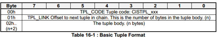
1个byte的TPL_CODE,类似于ID
1个byte的LEN
不定长的tuple body,但是不超过255
Tuple code list如下图
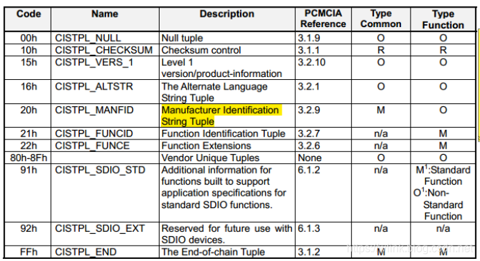
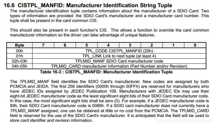
我们还是只拿一个制造商tuple code来说明下,让你们大概知道tuple code是什么就足够了吧
智能推荐
【WebApi】————.net WebApi开发(一)_webapi .net-程序员宅基地
文章浏览阅读8.5k次。【1】.部署环境.net4及以上版本。【2】.vs2010 开发需单独安装vs2010 sp1和mvc4mvc4:http://www.asp.net/mvc/mvc4【3】.开发1.新建项目选择ASP.net MVC 4 Web应用程序2.选择Web API 3.在新建立的项目里面有已经生成的webapi模版其中App_Start文件夹下WebApiCo..._webapi .net
几招教你阻止百度搜索自动跳转百度APP(其他网站也适用)!_百度自动跳转app怎么解决-程序员宅基地
文章浏览阅读10w+次,点赞15次,收藏33次。最近阿虚看到个消息说「百度」发布了新政策,禁止网站通过搜索引擎打开后折叠内容强迫下载APP客户端听起来似乎是百度难得良心一回?但实际上该政策仅限于手机百度APP内如果你是通过浏览器用百度搜索则与新政策完全没关系正好前不久不少粉丝来问过我这样一个问题:怎么屏蔽手机浏览器上的「跳转某某APP打开查看」提示那今天阿虚就来教一下怎么解决吧,毕竟这东西的确是有点烦人…屏蔽「跳转某某APP打开查看」这个问题我细看了下,还得分俩类:文章只能显示部分,然后提示你需要安装APP才能查看的,这种应该是大_百度自动跳转app怎么解决
PHP快速入门12-异常处理,自定义异常、抛出异常、断言异常等示例_php 抛出异常-程序员宅基地
文章浏览阅读843次。PHP的异常处理机制可以帮助我们在程序运行时遇到错误或异常情况时,及时发出警告并停止程序继续运行。下面是10个例子,分别展示了PHP异常处理的不同用法。_php 抛出异常
linux 清空docker容器日志_linux清理docker容器log-程序员宅基地
文章浏览阅读221次。【代码】linux 清空docker容器日志。_linux清理docker容器log
青岛大学开源OJ平台搭建_github oj开源-程序员宅基地
文章浏览阅读7.3k次,点赞3次,收藏15次。源码地址为:https://github.com/QingdaoU/OnlineJudge可参考的文档为:https://github.com/QingdaoU/OnlineJudgeDeploy/tree/2.0一、安装所依赖的环境sudo apt-get update && sudo apt-get install -y vim python-pip curl g..._github oj开源
浅谈数据安全-程序员宅基地
文章浏览阅读4.4k次。在《网络安全法》中,虽然已经明确了要求保障网络数据的完整性、保密性、可用性的能力,但随着近些年数据安全热点事件的出现,如数据泄露事件、个人信息滥用事件。表明对数据保护的要求仅依赖《网络安全法》中的几款条例是不足以支撑的。因此2021年9月1日《中华人民共和国数据安全法》便正式诞生,从此数据安全也被推上了风口浪尖。那么数据安全如何定义?与传统网络安全有何区别?数据安全体系又应该如何建立?..._数据安全
随便推点
联想笔记本G510升级固态硬盘(SSD)血泪教程!!!_联想g510更换固态硬盘-程序员宅基地
文章浏览阅读8.5w次,点赞23次,收藏55次。#联想笔记本G510升级固态硬盘(SSD)血泪教程!!!用了5年的联想笔记本G510,经过了四年的游戏历程,然后四年后还老当益壮的挣扎在我工作的战斗一线,是我并肩作战多年,比兄弟还要亲的兄弟,虽然此时已经身躯残破,反应迟缓我依旧不舍得抛弃它(主要是没钱!)然后为了我个人的用户体验决定花少量的票子,让它多挣扎一会,最好是能坚持到我度过贫困期. 下面是我升级的悲催历程! - 首先为了提升运行速..._联想g510更换固态硬盘
问题记录——正则表达式匹配控制符_正则表达式匹配控制字符-程序员宅基地
文章浏览阅读910次。问题前端用xterm.js通过websocket连接docker虚拟终端,返回的字符中包括如下字符串,其中有两个控制字符,“ESC"和"BEL” ,想通过正则表达式匹配这一段字符,然后去掉这段字符:参考文档控制字符编码表转义符对照表通过上面查询得知,"ESC"和"BEL"这两个控制符的ASCII码分别为:十进制为27和7,十六进制为0x1B和0x07,转义符分别为:\e和\a代码**注意:**直接使用ASCII码匹配是不行的,一定要用转义符才行。如下测试代码中,只有regex3才能匹_正则表达式匹配控制字符
Android RIL框架分析-程序员宅基地
文章浏览阅读1.5k次。1.RIL框架 RIL,Radio Interface Layer。本层为一个协议转换层,提供Android Telephony与无线通信设备之间的抽象层。 Android RIL位于Telephony Frameworks之下,Modem之上的,根据源码,RIL可以分为两个部分:Frameworks 框架层中的java程序,简称RILJ。HAL层中C/C++程序,简称RILC,RILC具体的又包括LibRIL、Rild和Reference-RIL这三个部分。 Andr..._ril框架
Python编程基础:第六节 math包的基础使用Math Functions_ps math function-程序员宅基地
文章浏览阅读565次。第六节 math包的基础使用前言实践前言我们通常会对数值型变量进行计算,这里我们给出一些常用的函数用于辅助你的计算过程。常用的数学计算函数均在math包。实践首先我们导入math包,并定义一个浮点型变量pi将其赋值为3.14:import mathpi = 3.14如果我们需要计算浮点型变量四舍五入后的计算结果,用函数round()即可:print(round(pi))>>> 3如果我们需要向上取整,那就需要函数math.ceil():print(math.cei_ps math function
canal异常 Could not find first log file name in binary log index file_canal could not find first log file name in binary-程序员宅基地
文章浏览阅读4.4k次,点赞3次,收藏2次。Could not find first log file name in binary log index file问题解决解决过程问题最近在使用canal来监测数据库的变化,处理变动的数据。由于有一段时间没有用了,这次启动在日志文件中看到这个异常 Could not find first log file name in binary log index file,详细信息如下:2020-12-16 19:14:42.053 [destination = tradeAndRefund , addr_canal could not find first log file name in binary log index file
【练习】生成10个1到20之间的不重复的随机数并降序输出-程序员宅基地
文章浏览阅读960次。分析:1.创建一个Random对象;2.创建一个hashset的集合对象;3.循环生成10个1-20的随机数4.输出。package edu.xalead;import java.util.*;public class Test { public static void main(String[] args) { Random r...